|
|
EOTRON | About Us | Technology | Products | Contact Us |
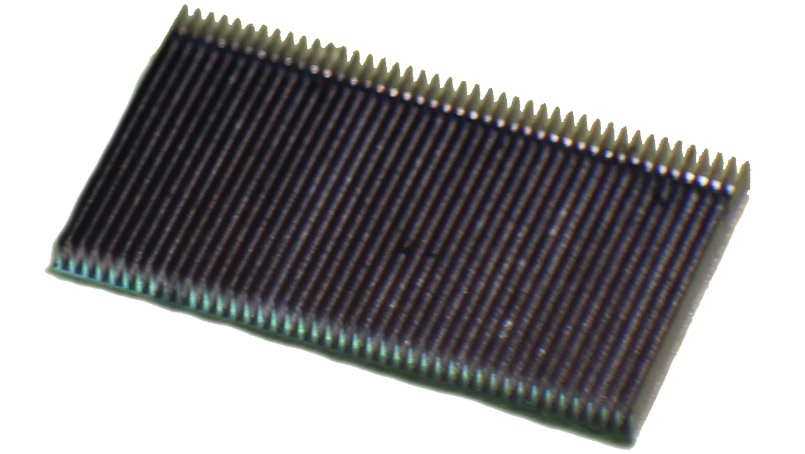
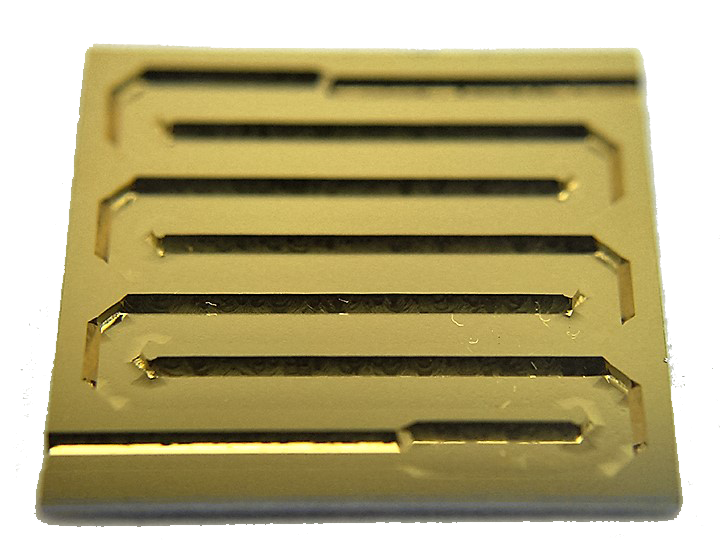
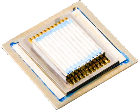
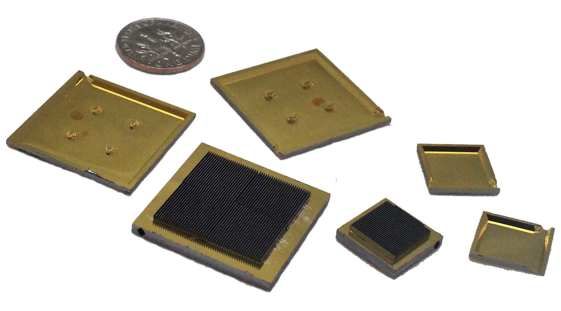
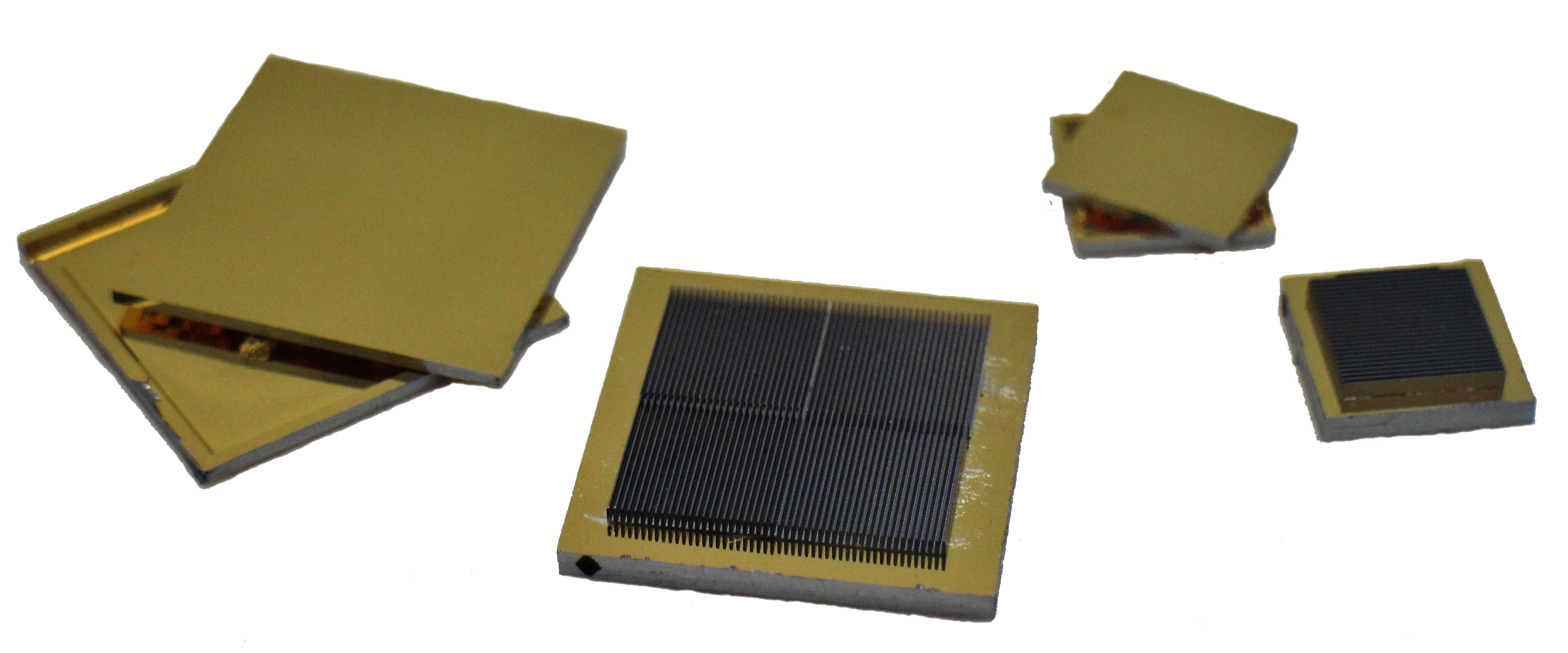
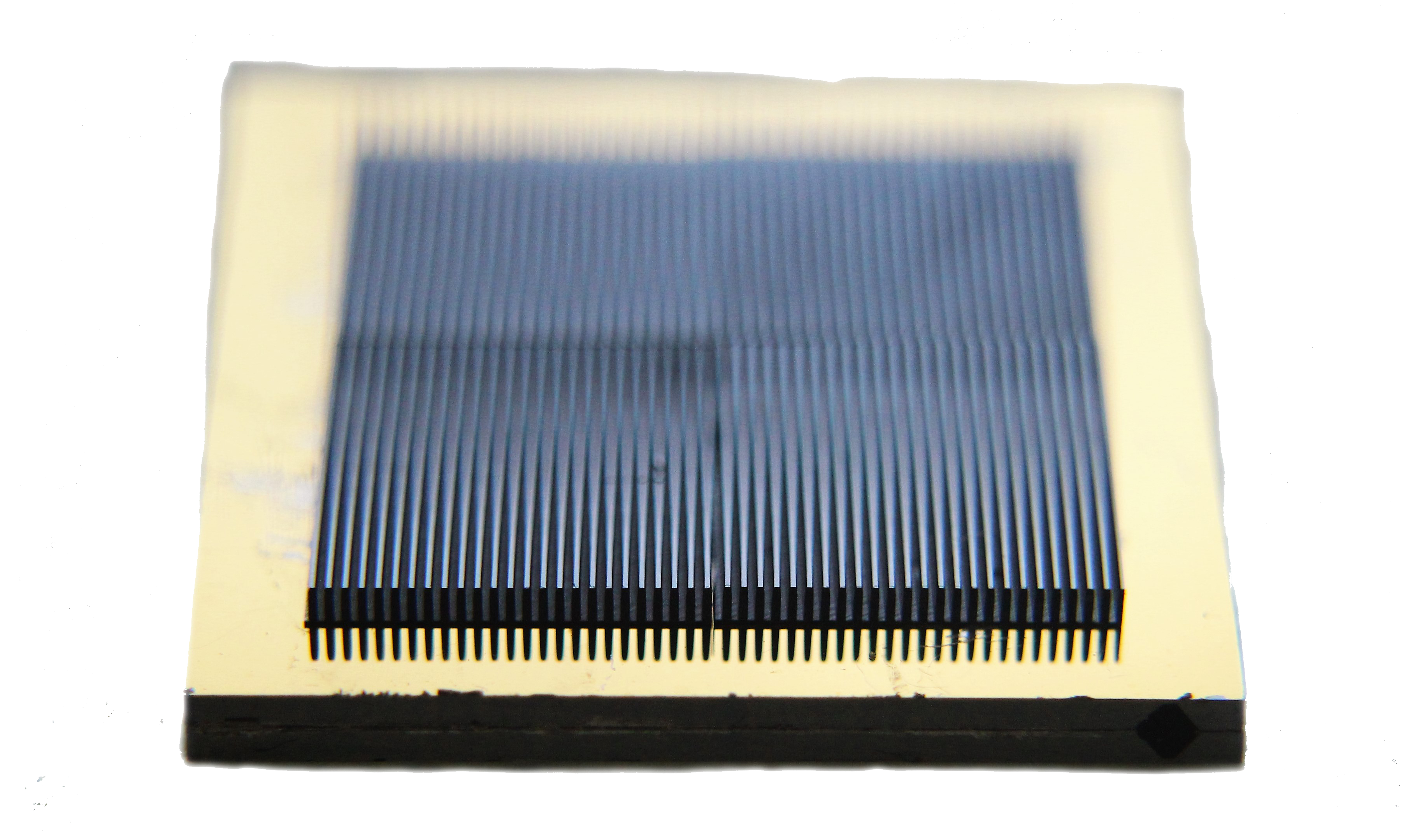
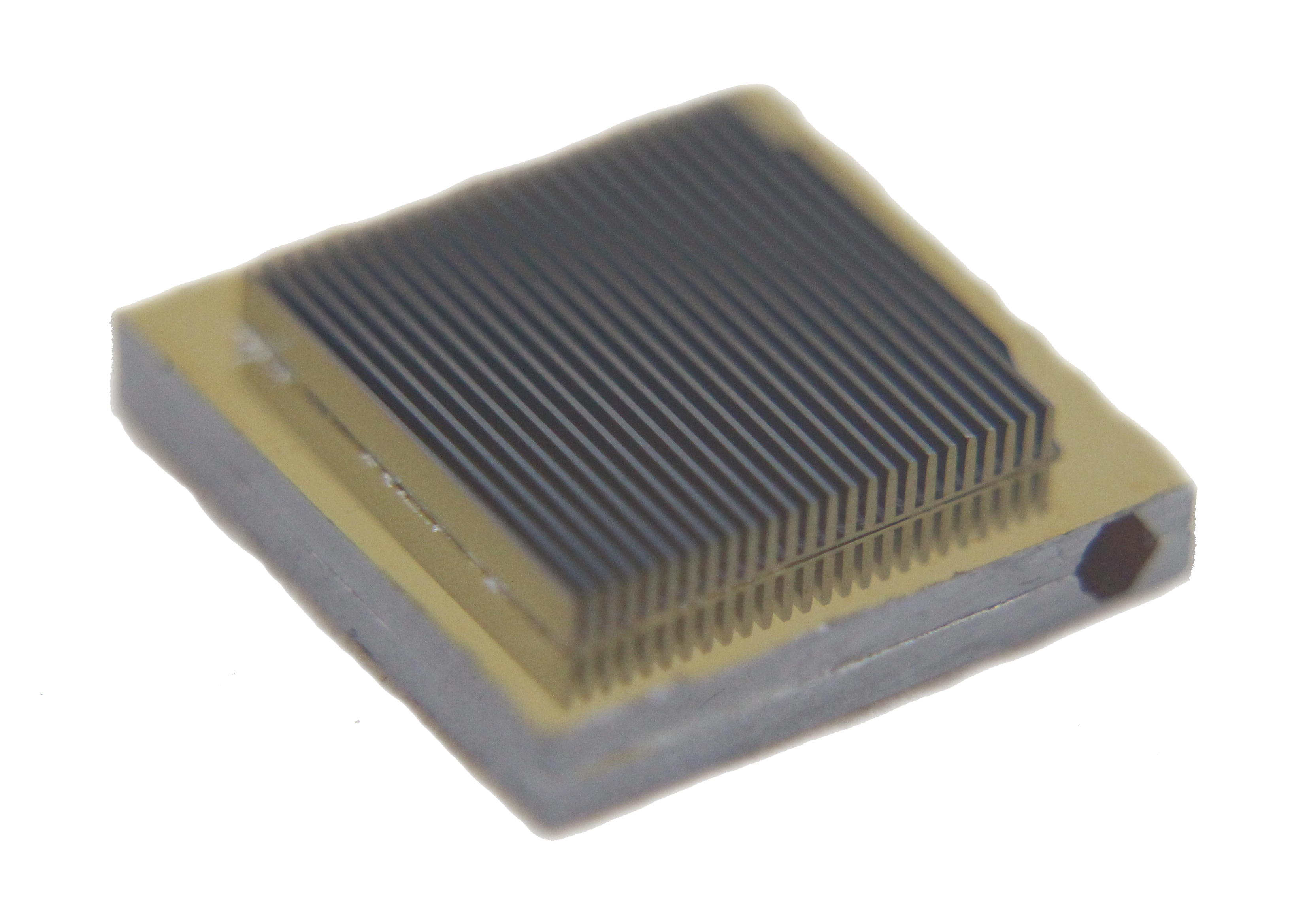
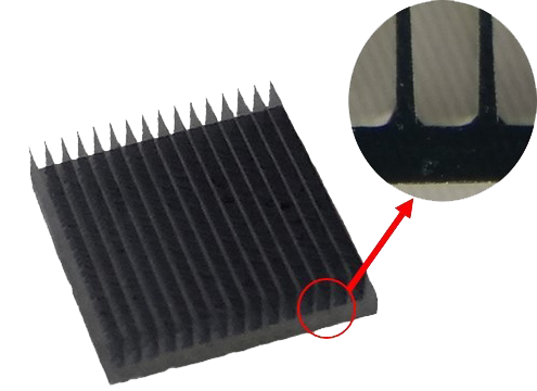 Eotron’s Silicon Heatsink is designed to replace compact
copper or aluminum heatsinks where the size, space and efficiency of
the heatsink is crucial. Our Silicon Heatsink delivers 5 to 10 times
more fin-surface area than metal heatsinks of the same size due to
silicon’s ability to fabricate more fins and as thin as
10μm in size.
Eotron’s Silicon Heatsink is designed to replace compact
copper or aluminum heatsinks where the size, space and efficiency of
the heatsink is crucial. Our Silicon Heatsink delivers 5 to 10 times
more fin-surface area than metal heatsinks of the same size due to
silicon’s ability to fabricate more fins and as thin as
10μm in size.
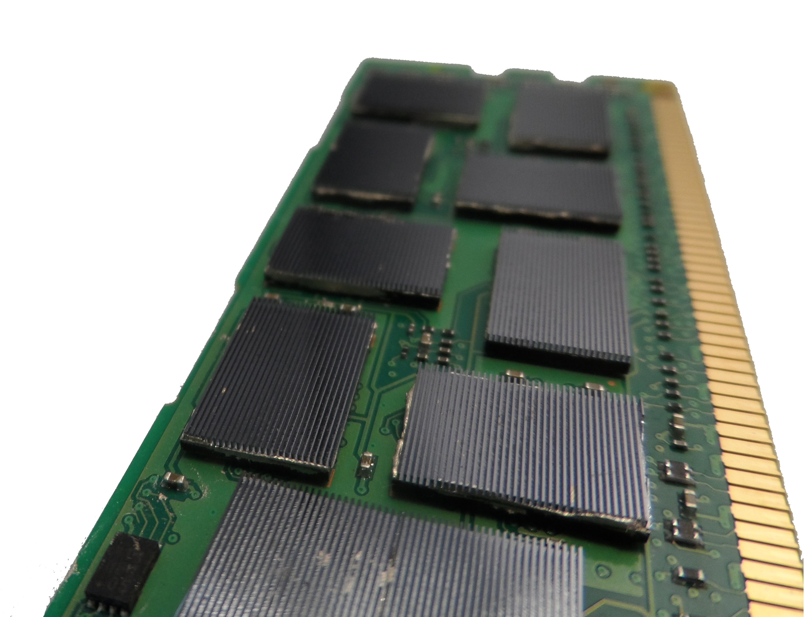
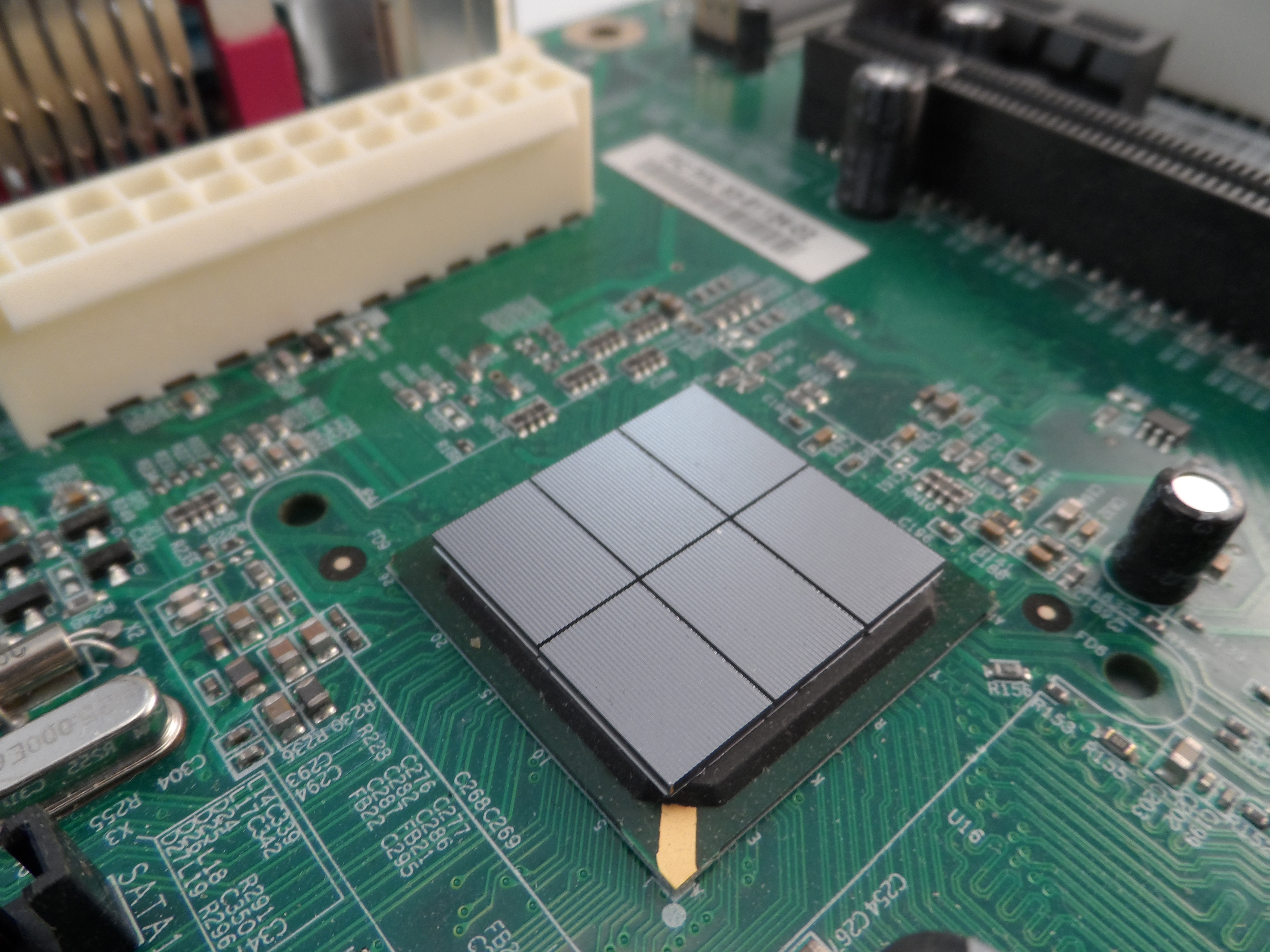
Silicon Heatsinks can be used in a convective cooling or forced-air
cooling configuration. Depending on the heat dissipation
configuration, the base of the Silicon Heatsink can be soldered,
epoxied or attached using various thermal compounds directly to any
silicon IC chip or PCB.
Our proprietary fabrication techniques produced the most efficient
heatsink designs (patented) while using a bulk low-cost process.
| Standard Heatsink Size | 10mm(L) x 10mm(W) x 1.2mm(H) |
| Silicon Heatsink Base Thickness | >0.2 to 0.3mm |
| Silicon Fin Thickness | 30 to 75μm tapered shape (US Patent) |
| Silicon Fin Pitch | 0.3 to 0.5mm depending on forced-air or not |
| Surface Finish | Less than 0.1μm |
| Special Enhancements |
|
*** Custom size and fin design is also available.
|
|
|
Please contact us for further information at sales@eotron.com.
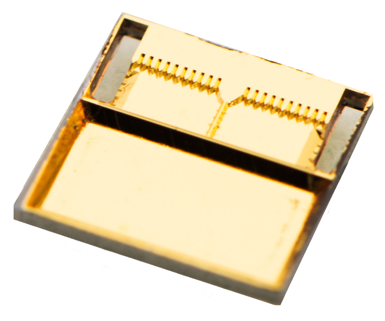
 Eotron’s Silicon Cold Plate was designed to replace copper or
aluminum metal cold plates with silicon to provide better cooling
efficiency, form-factor and thermal expansion match with silicon IC
chips. Any IC chip can be mounted directly on the Silicon Cold Plate
with electrical layout printed on the surface of SCP allowing the
lowest thermal resistance from IC chip to liquid channel embedded in
the SCP.
Eotron’s Silicon Cold Plate was designed to replace copper or
aluminum metal cold plates with silicon to provide better cooling
efficiency, form-factor and thermal expansion match with silicon IC
chips. Any IC chip can be mounted directly on the Silicon Cold Plate
with electrical layout printed on the surface of SCP allowing the
lowest thermal resistance from IC chip to liquid channel embedded in
the SCP.
The greatest advantage of the SCP product is delivering coolant
directly underneath of high thermal load IC chips and without any
thermal expansion mismatch. The SCP can be bonded to an PCB with
solder bumps further isolating high thermal load ICs from those
devices sensitive to heat.
Our Silicon Cold Plate has proven to deliver more than 80
watts/cm2 of heat dissipation in the smallest form factor
of any cold plate design and SCP has a lower fouling factor than
metal cold plate designs due to non-oxidation and non-chemical
reacting physical property of silicon. Both surfaces of the SCP can
be printed with electrical layout to bond IC chips reducing thermal
resistance to a minimum.
| Silicon Cold Plate Size | Up to 70mm(L) x 70mm(W) x 2mm or 4mm(H) |
| Inlet and Outlet Port Size | >1.59mm (1/16") or 3.175mm (1/8") |
| Heat Dissipation | Up to 80 watts/cm2 (1.59mm tubing) |
| Flow Rate | 0.25 liter/minutes (for 1.59mm tubing) |
| Maximum Pressure | Up to 1034 Kilopascal (150 PSi) |
| PCB Layout | Single layer, 0.1mm features |
| Advantages |
|
|
|
|
Please contact us for further information at sales@eotron.com.
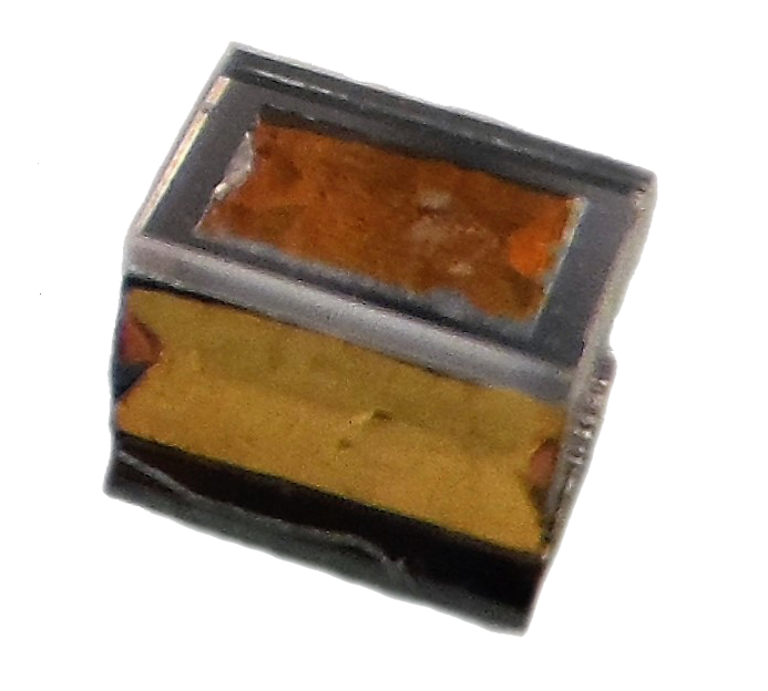
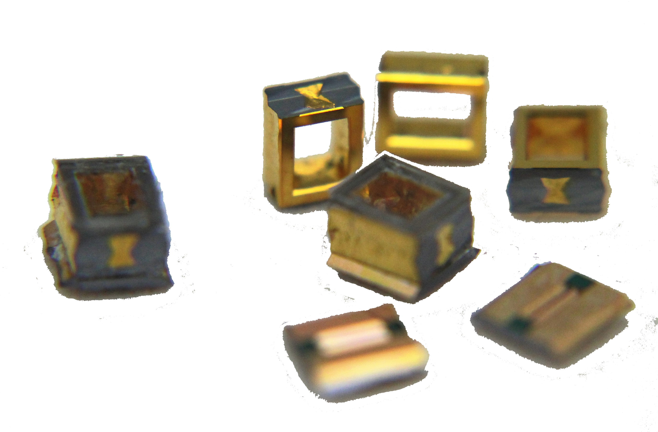
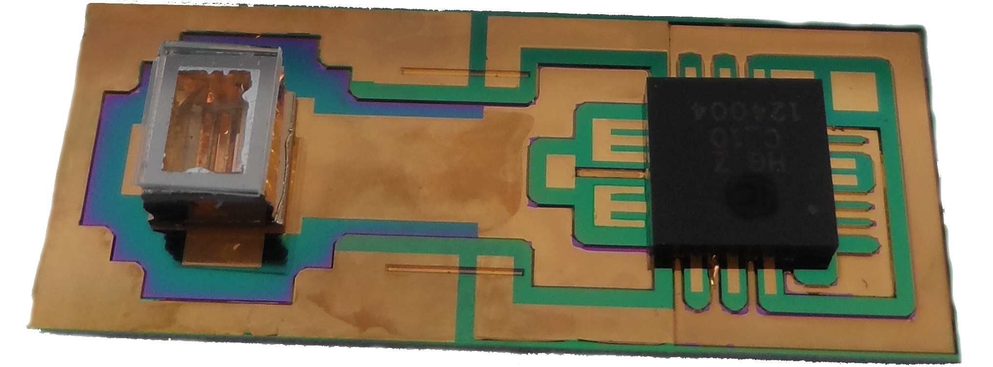
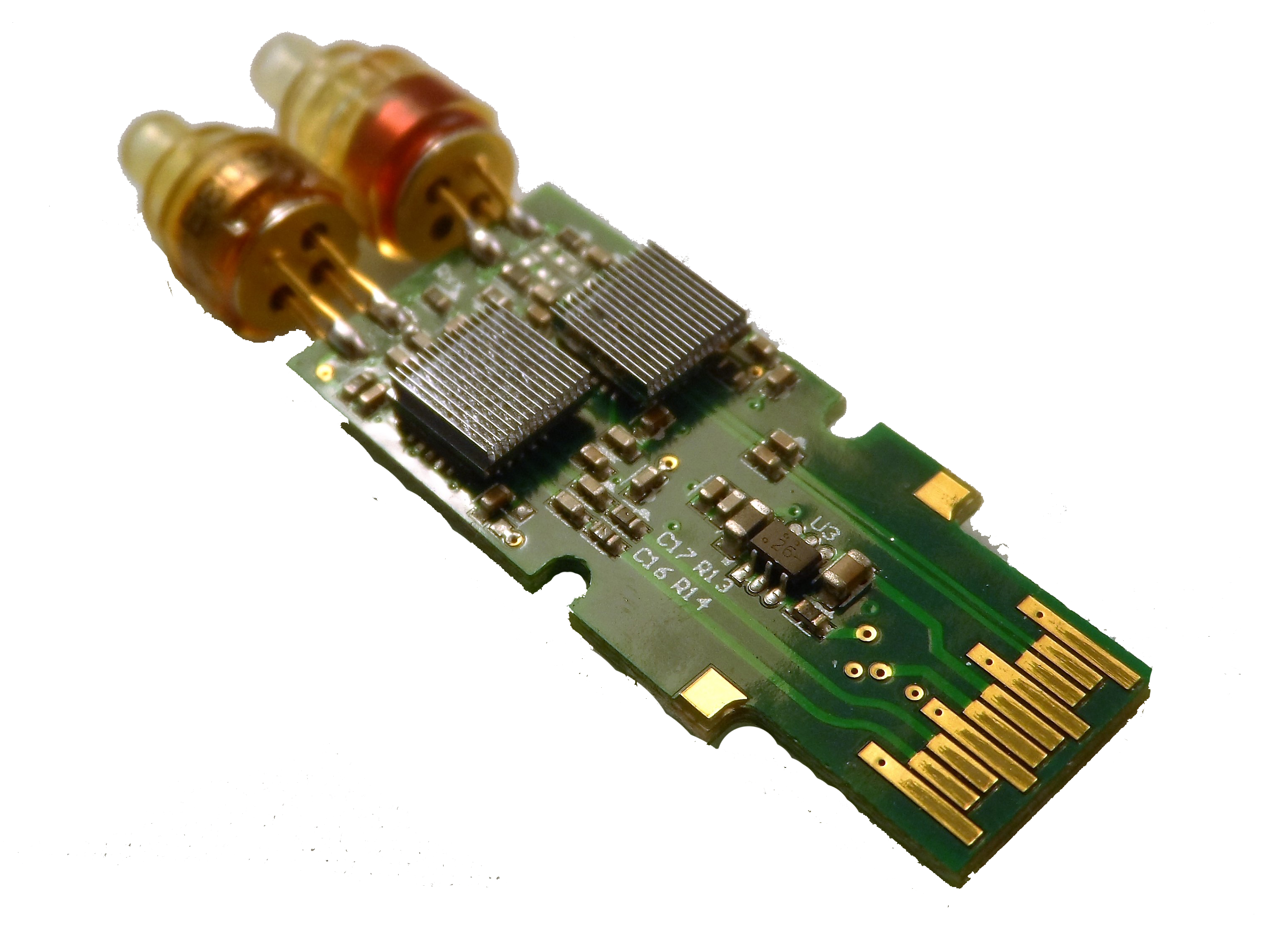
 Eotron’s all Silicon TO-Can package is designed to replace a
conventional optical metal TO-Can packages. This package was
designed to improve thermal conductivity and lower production cost.
The Silicon TO-Can package consists of three separate silicon
components and an optical window to package any small photonic
device such as edge-emitting Laser Diodes, VCSELs, UV LEDs or high
power LEDs. Each silicon component and window are bonded together to
seal the light source.
Eotron’s all Silicon TO-Can package is designed to replace a
conventional optical metal TO-Can packages. This package was
designed to improve thermal conductivity and lower production cost.
The Silicon TO-Can package consists of three separate silicon
components and an optical window to package any small photonic
device such as edge-emitting Laser Diodes, VCSELs, UV LEDs or high
power LEDs. Each silicon component and window are bonded together to
seal the light source.
Among the advantages of our Silicon TO-Can package is eliminating
wire-bonding by direct bonding of the device and flip-chip bonding
of TO-Can package to improve thermal dissipation. No wire-bonding
and better thermal dissipation and lower circuit inductance allows
the device to operate at high frequency and higher peak power
operation.
Wafer Scale assembly of the silicon package and device using Pick
and Place robots allow high volume production and lower
manufacturing cost.
| Current Silicon TO Can Package Size | 4.3mm(L) x 3.2mm(W) x 3.0mm(H), custom design available |
| Illumination Source | Edge-emitter lasers, VCSEL, LED |
| Heat Dissipation | Up to 1 watt (with silicon heatsink) |
| Protective Window | Glass or quartz window (Passive alignment possible) |
| Advantages |
|
|
|
|
Please contact us for further information at sales@eotron.com.
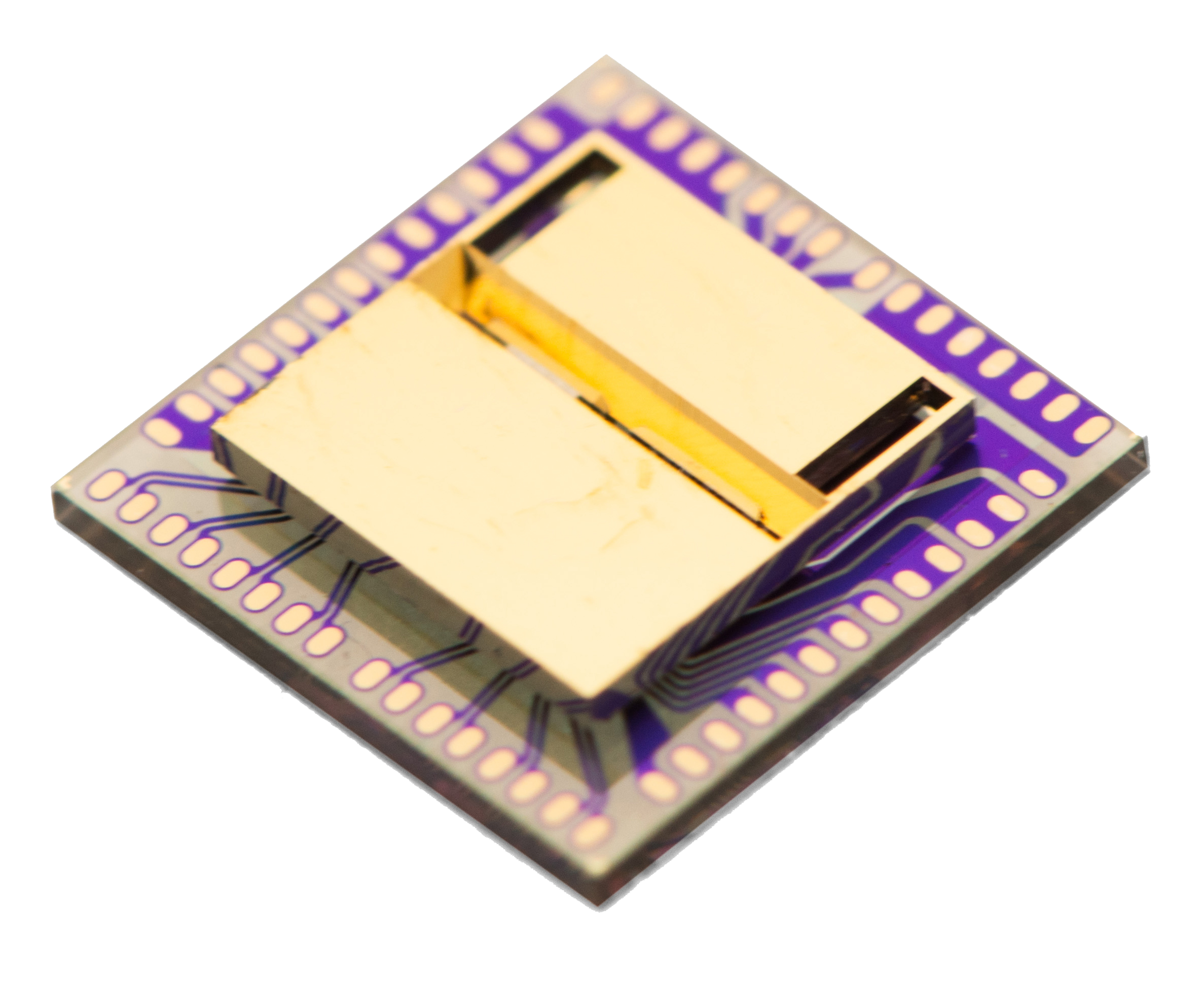
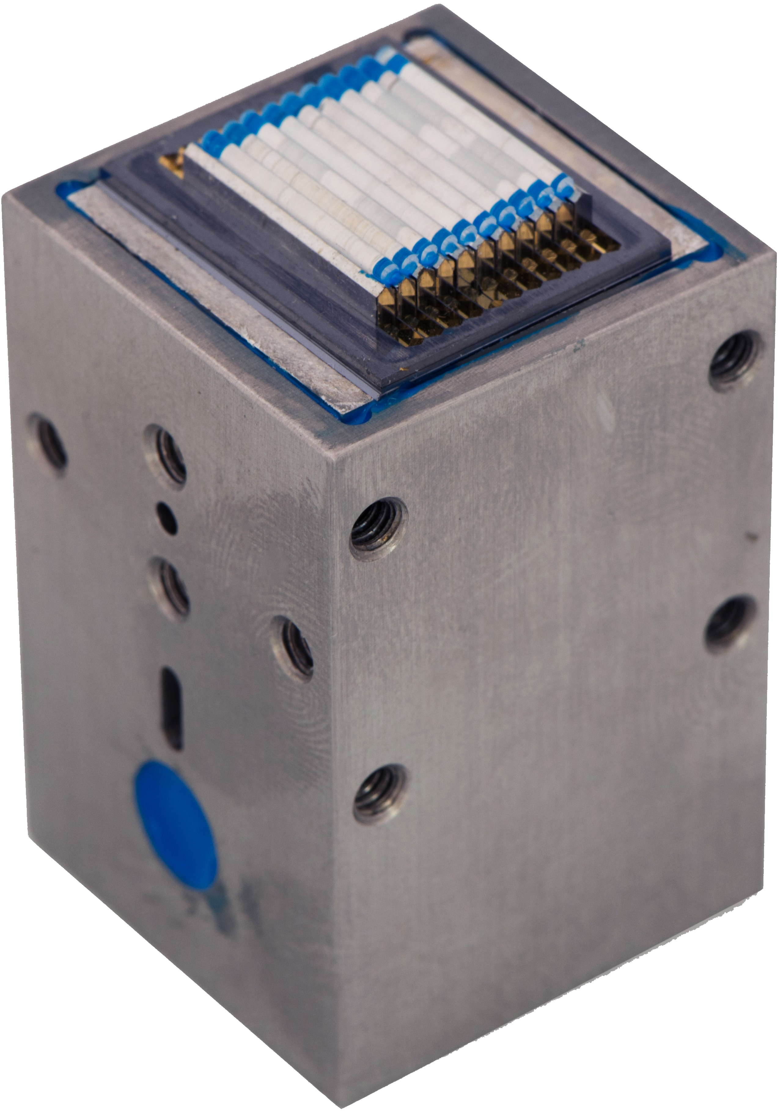 Eotron’s Patented Silicon-based Laser packaging was designed
to mount multiple high power diode bars (Stacks) in a liquid cooled
configuration. Laser Diode Bars are bonded to each side of our
proprietary Silicon Fins in a 1-bar, 2-bar, 5-bar or 10-bar
configuration using soft-solder. Each Silicon Fin has internal
’Macro’ water channels so each Diode Bar is individually
cooled. The package consists of silicon-base, silicon-spacer and
silicon-fins to assembly any 1mm x 10mm or 2mm x 10mm laser diode
bar.
Eotron’s Patented Silicon-based Laser packaging was designed
to mount multiple high power diode bars (Stacks) in a liquid cooled
configuration. Laser Diode Bars are bonded to each side of our
proprietary Silicon Fins in a 1-bar, 2-bar, 5-bar or 10-bar
configuration using soft-solder. Each Silicon Fin has internal
’Macro’ water channels so each Diode Bar is individually
cooled. The package consists of silicon-base, silicon-spacer and
silicon-fins to assembly any 1mm x 10mm or 2mm x 10mm laser diode
bar.
Our liquid cooled silicon diode stack maximizes brightness in a 10mm
x 10mm active area, emitting up to 1 kW, and the silicon laser
package delivers a thermal resistance of less than 0.1°C/watts
in 10mm2 area.
Due to a special tooling requirement and assembly techniques, a
sub-assembled silicon laser package can be purchased for your
application.
| Silicon Laser Package Configuration | Single bar, 2-bar, 5-bar or 10-bar |
| Diode Bar Configuration | 1mm x 10mm or 2mm x 10mm |
| Diode Bar Thickness | 120 to 130 μm (Required to adjust diode package pitch) |
| Diode Bar-to-bar Pitch | 1mm (nominally) |
| Liquid Flow Channel Design | Macro-channel (>1mm2 cross-section) |
| Water Flow-rate | 11 liters/minute |
| FAC and SAC Lens Requirements |
FAC lens: Passive alignment onto the stack SAC lens: Silicon SAC mounting structure available |

|

|
|
Please contact us for further information at sales@eotron.com.
 Eotron’s Silicon Heat Reservoir (SHR) is based on the concept
of absorbing waste heat using Phase-Change-Material (PCM) to slowly
absorb and dissipate heat over time, smoothing out thermal loading
in a pulsed operation. Our Silicon Heat Reservoir (SHR) is
constructed using mono-crystal silicon to spread heat in a PCM
silicon filled container, allowing waste heat to efficiently migrate
from the heat source to the PCM. The SHR allows a device to maintain
operating temperatures slightly below the melting temperature of PCM
until it reaches saturation. Typically, PCM expands thermal capacity
by a factor of 5 to 8 times more compared to other solid thermal
materials.
Eotron’s Silicon Heat Reservoir (SHR) is based on the concept
of absorbing waste heat using Phase-Change-Material (PCM) to slowly
absorb and dissipate heat over time, smoothing out thermal loading
in a pulsed operation. Our Silicon Heat Reservoir (SHR) is
constructed using mono-crystal silicon to spread heat in a PCM
silicon filled container, allowing waste heat to efficiently migrate
from the heat source to the PCM. The SHR allows a device to maintain
operating temperatures slightly below the melting temperature of PCM
until it reaches saturation. Typically, PCM expands thermal capacity
by a factor of 5 to 8 times more compared to other solid thermal
materials.
This silicon structure is designed to maintain device temperature
under certain heat loading conditions. Optimizing the design of the
silicon structure is needed to manage the overall thermal
performance of the heat source under variable ambient conditions.
The design of SHR can be optimized according to customer needs and
application requirements.
| Silicon Heat Reservoir Size | 30mm(L) x 30mm(W) x 2mm(H), (custom designs available) |
| Heat Capacity | A few watts per centimeter squared heat density |
| Advantages |
|
|
|
|
Please contact us for further information at sales@eotron.com.
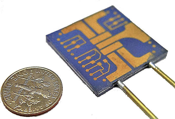
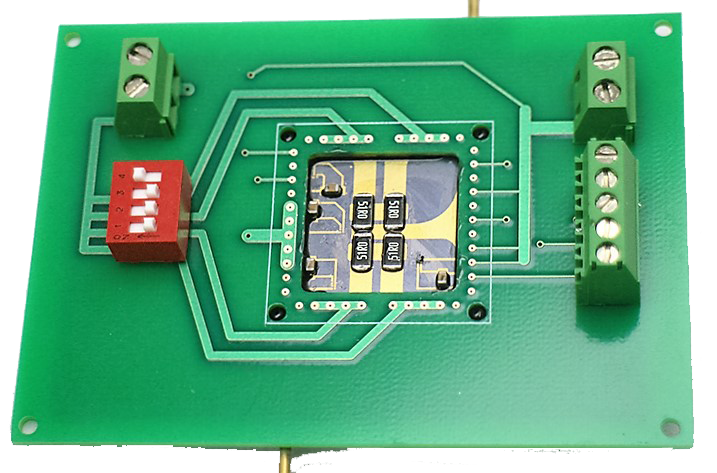
 Eotron’s Silicon Thermal Isolator (STI) is based on a concept
of separating the thermal path between a high heat producing device
and an adjacent temperature sensitive device. The specially designed
and patented silicon structure allows separation of any heat
generating device to a device which may be sensitive to temperature.
Eotron’s Silicon Thermal Isolator (STI) is based on a concept
of separating the thermal path between a high heat producing device
and an adjacent temperature sensitive device. The specially designed
and patented silicon structure allows separation of any heat
generating device to a device which may be sensitive to temperature.
Our Silicon Thermal Isolator works as a heat spreader along with a
special patented structure added to the silicon, which isolates the
thermal ground for each IC chip. Most designs also use the
electrical ground as the thermal ground. This results in all heat
generating devices (IC chips) mounted on PCB to experience higher
junction temperatures due to the temperature rise in the ground
plane. Our Silicon Thermal Isolator (STI) mounted on the heat
generating and adjacent heat-sensitive devices improves the
performance and life-time of all devices. Also, a STI can be used as
a silicon interposer with heat separating structure embedded in the
interposer. Data shows the STI can achieve more than 10 degrees of
temperature difference between two different areas in single Silicon
Thermal Isolator.
We can provide more specific information depending on your
application.
| Silicon Thermal Isolation Size | 30mm(L) x 30mm(W) x 1mm(H), (custom designs available) |
| Temperature Separation | 10 °C or more |
| Advantages |
|
|
|
|
Please contact us for further information at sales@eotron.com.