ABOUT EOTRON
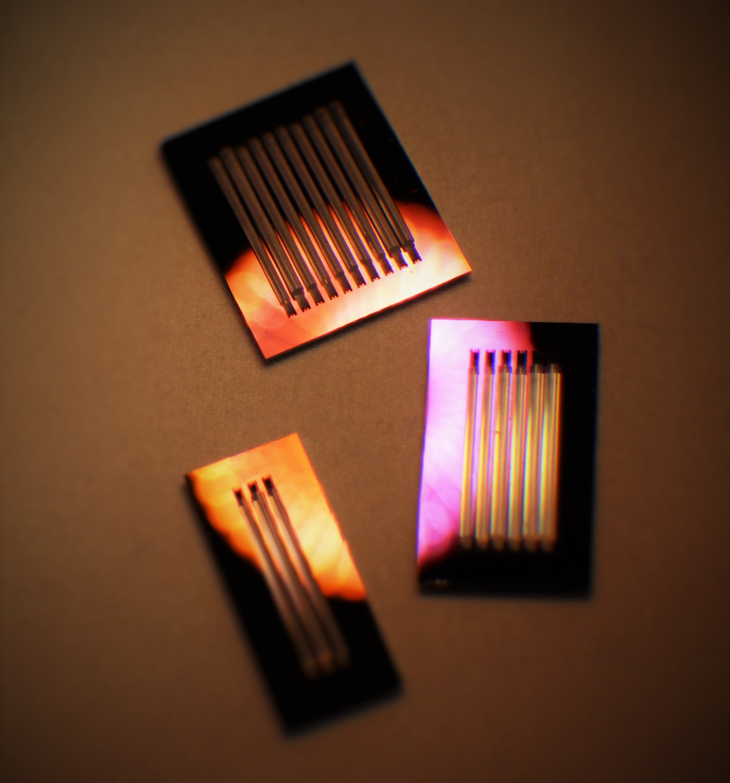
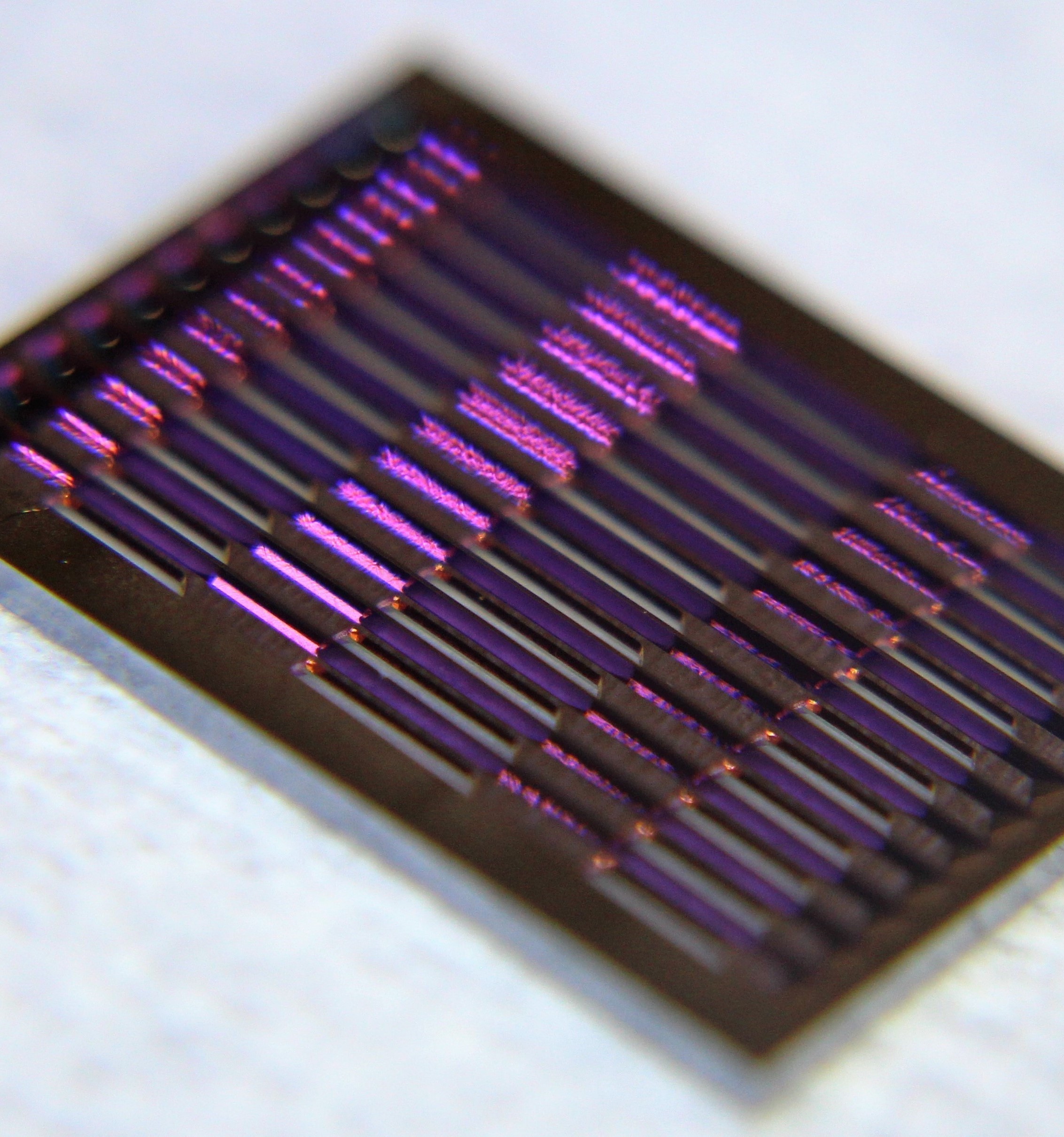
 Eotron LLC was founded in 2006 primarily to develop a compact DPSS
laser using a silicon substrate to contain all pump diodes and optical
mounts on one silicon based MEMS bench. The main challenge in building
this silicon-bench was dissipating the large amount of waste heat from
the pump diodes and solid-state crystal. It was also very challenging
to integrate all the optical components using a 2D configuration while
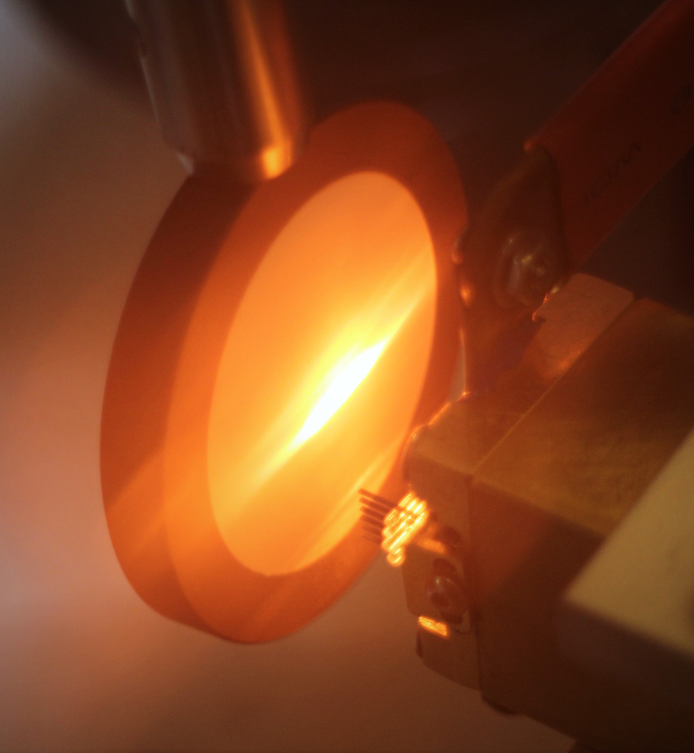
removing all of the waste heat. Therefore, a configuration using a 3D
Silicon structure containing a high power diode stack was conceived,
designed, fabricated and tested in 2011.
Eotron LLC was founded in 2006 primarily to develop a compact DPSS
laser using a silicon substrate to contain all pump diodes and optical
mounts on one silicon based MEMS bench. The main challenge in building
this silicon-bench was dissipating the large amount of waste heat from
the pump diodes and solid-state crystal. It was also very challenging
to integrate all the optical components using a 2D configuration while
removing all of the waste heat. Therefore, a configuration using a 3D
Silicon structure containing a high power diode stack was conceived,
designed, fabricated and tested in 2011.
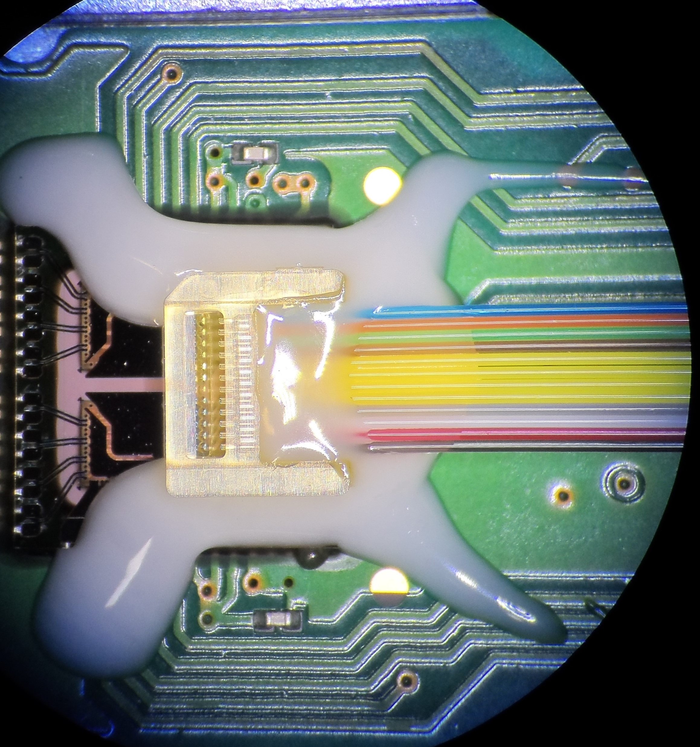
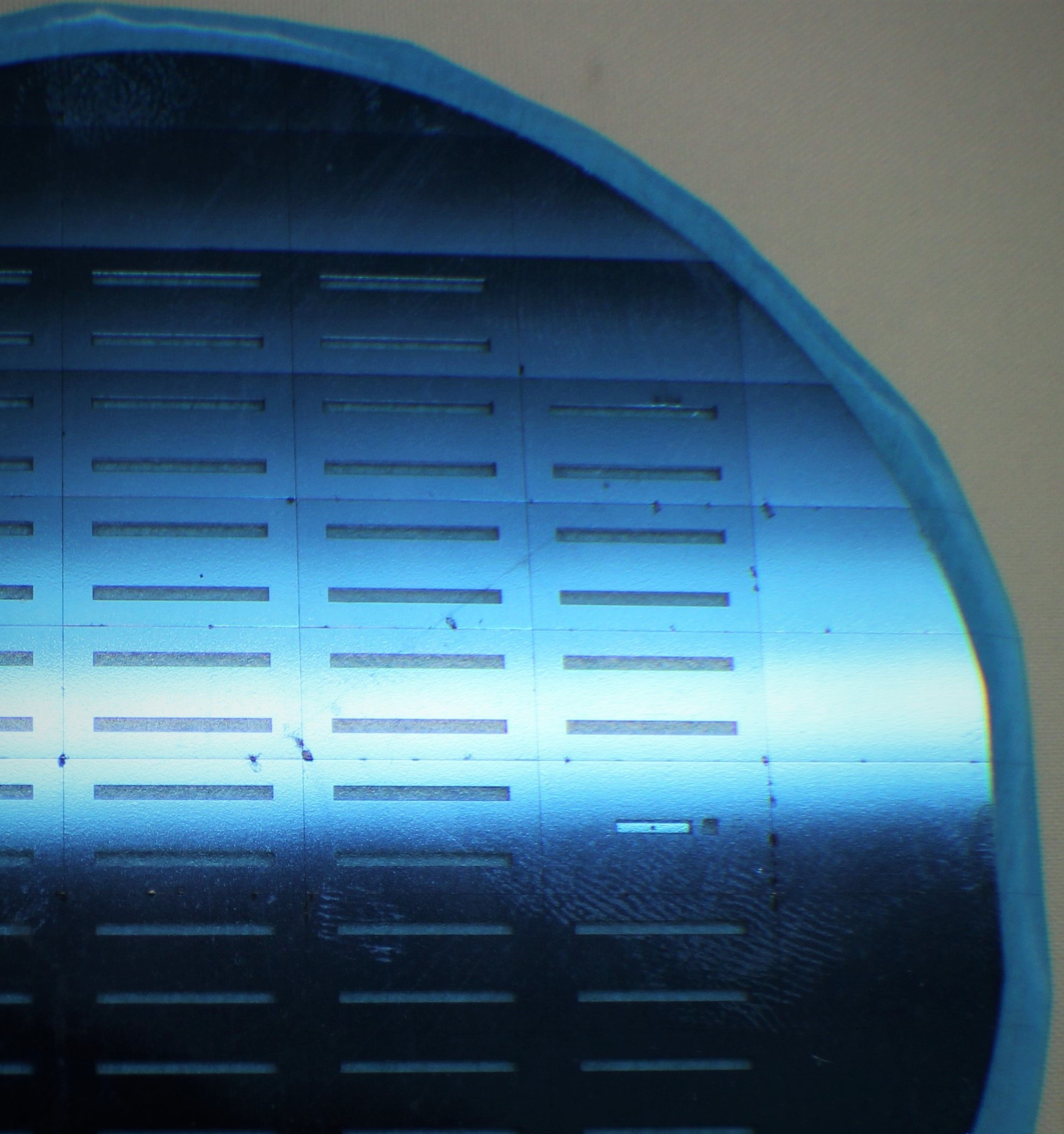
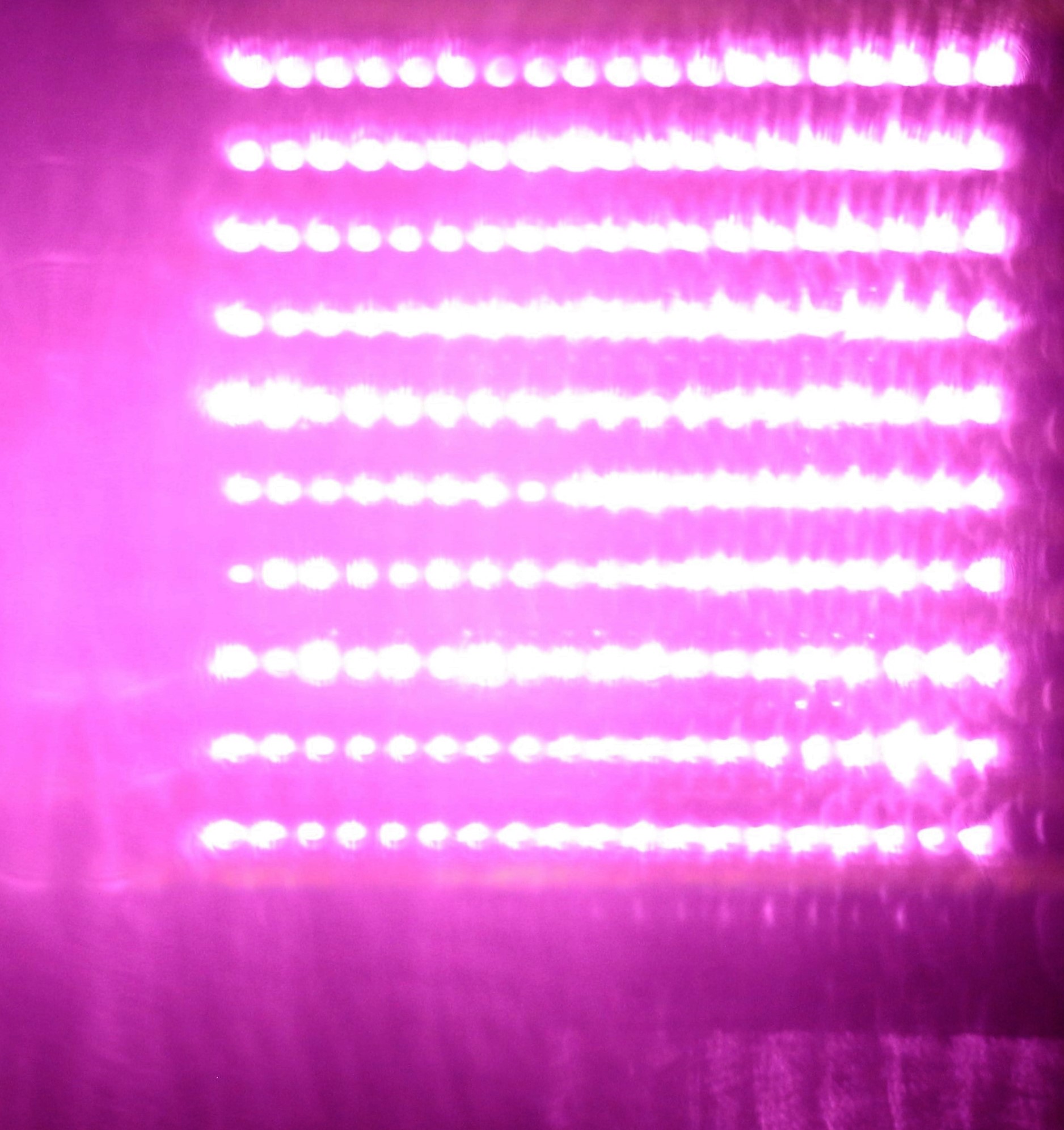
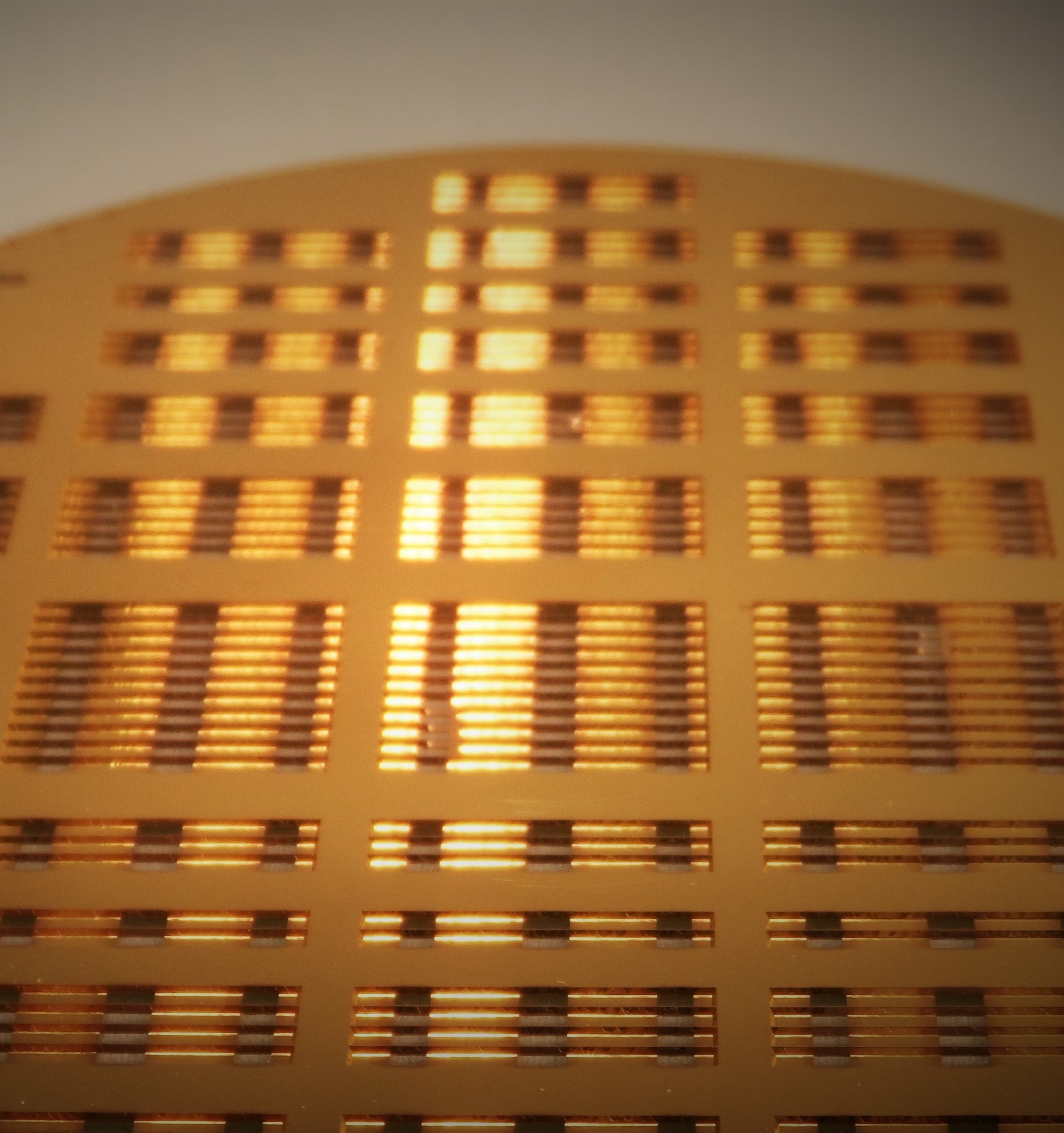
The resulting high power silicon diode laser stack was further
developed in 2012 using an improved 3D silicon structure and a number
of proprietary Silicon MEMS fabrication processes. All techniques and
patents were developed under private funding. Based on these
accomplishments, Eotron was awarded with several SBIR Phase 1 and
Phase 2 contracts from the Air Force, Missile Defense Agency, Navy and
NASA to develop new concepts in cooling high power lasers and other
electronic devices and systems.
Building on the technology and continued research, Eotron expanded its
offering to include 3D Silicon components, designs and techniques
aimed at improving thermal management of both electronic and photonic
devices with high thermal flux. These designs, components and
expertise have led to interest and development projects from the
commercial marketplace, including from leading Fortune 100 companies.
Eotron currently has over 20 awarded patents related to active and
passive cooling using 2D and 3D silicon structures, with another 20 or
more pending.
Eotron is located in Oceanside, CA, where it maintains a 4500 sq. ft
facility with engineering labs and class 10,000 clean room. The
company leases access to a silicon wafer fabrication MEMS facilities
in US, staffed by Eotron employees, with volume production handled by
dedicated silicon foundry suppliers with world-wide locations.